Joint press release by Hokkaido University, Japan, and Lund University, Sweden.
Nanostructured two-dimensional gold monolayers offer possibilities in catalysis, electronics, and nanotechnology.

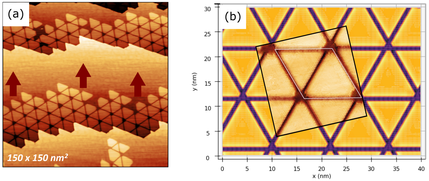
Scanning-tunnelling microscopy (STM) image illustrating the formation of nanostructuring in the gold monolayer on iridium upon exposure to boron flux (a), and the theoretically obtained structure of this system, with the unit supercell indicated by a white rhombus, overlapped (black square) with its close-up atomically resolved STM image (b). (Alexei Preobrajenski, et al. Nature Communications. December 10, 2024)
Researchers have created nearly freestanding nanostructured two-dimensional (2D) gold monolayers, an impressive feat of nanomaterial engineering that could open up new avenues in catalysis, electronics, and energy conversion.
Gold is an inert metal which typically forms a solid three-dimensional (3D) structure. However, in its 2D form, it can unlock extraordinary properties, such as unique electronic behaviors, enhanced surface reactivity, and immense potential for revolutionary applications in catalysis and advanced electronics.
One of the challenges in synthesizing 2D gold monolayers has been stabilizing isotropic metallic bonds in strictly 2D forms. To address this, the research team at Lund University and Hokkaido University employed a novel bottom-up approach combined with high-performance computations, enabling the creation of macroscopically large gold monolayers with unique nanostructured patterns, remarkable thermal stability, and potential catalytic utility.
The team grew gold monolayers on an iridium substrate and embedded boron atoms at the interface between gold and iridium. This innovative technique produced suspended monoatomic sheets of gold, which had a hexagonal structure with nanoscale triangular patterns. Incorporating boron enhanced the stability and structural integrity of the gold layers, allowing the nanostructures to form.
"The ease of preparation and thermal stability of the resulting gold films is significant, making them a practical platform for further studies of fundamental properties of elemental 2D metals and their potential for diverse applications in electronics and nanotechnology," explains Dr. Alexei Preobrajenski of the MAX IV Laboratory, Lund University, and a corresponding author of the study.
Advanced characterization techniques, including scanning tunneling microscopy (STM) and X-ray spectroscopy, were employed to investigate the structural and electronic properties of the gold films. The analysis confirmed that embedding boron facilitates a transition from 3D to primarily 2D metal bonding, fundamentally altering the electronic behavior of the gold layers. This transformation underscores the unique nature of the synthesized films, as traditional methods typically fail to maintain a stable 2D metallic form, leading instead to small or unstable structures.
The ability to create stable and nearly freestanding metallic monolayers over a large area has far-reaching implications. "This research opens avenues for testing theories and further exploration into the potential applications of 2D metals in the various fields, including catalysis and energy conversion," says Associate Professor Andrey Lyalin of the Faculty of Science, Hokkaido University, and the other corresponding author of the study.
By addressing the challenges of stabilizing 2D metallic materials, this study contributes to the growing understanding of 2D materials and lays the groundwork for potential technological applications.
Original Article:
Alexei Preobrajenski, et al. Boron-Induced Transformation of Ultrathin Au Films into Two-Dimensional Metallic Nanostructures. Nature Communications. December 10, 2024.
DOI: 10.1038/s41467-024-54464-y
Funding:
This work was partly supported by the MEXT program: Data Creation and Utilization-Type Material Research and Development Project Grant Number JPMXP1122712807; the MEXT program for promoting researches on the supercomputer Fugaku: Data-Driven Research Methods Development and Materials Innovation Led by Computational Materials Science, JPMXP1020230327; and the Institute for Chemical Reaction Design and Discovery (ICReDD), established by the World Premier International Research Center Initiative (WPI). Calculations were performed using computational resources of the supercomputer Fugaku provided by the RIKEN Center for Computational Science (Project ID: hp230212); Institute for Solid State Physics, the University of Tokyo, Japan; and the Research Center for Computational Science, Okazaki, Japan (Project: 23-IMS-C016); MAX IV Laboratory for time on Beamline FlexPES under proposal 20200173 and MAX IV STM setup under proposal 20220019; Research conducted at MAX IV, a Swedish national user facility, is supported by the Swedish Research council under contract 2018-07152, the Swedish Governmental Agency for Innovation Systems under contract 2018-04969, and Formas under contract 2019-02496; Diamond Light Source for time via the in-house beam time allotment of Beamline I09.


