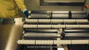
On most operating days, utitlisation operators carefully lower mirror-like cylindrical silicon ingots into the OPAL multi-purpose reactor.
They are handling silicon, one of the purest substances and perfect materials on the planet, with great precision and care. It remains in the reactor anywhere from a few hours to several days to undergo a process known as neutron transmutation doping (NTD) that will create the desired electrical properties for industry customers.
In the reactor, irradiation converts some of the silicon atoms into phosphorous which is the dopant in the silicon. The phosphorous atoms introduce free electrons into the crystal lattice to enhance conductivity. The more phosphorus, the more free electrons, the more electrically conductive the material becomes.
The mirror-like silicon ingots are transferred to the service pool for 48 hours until the radioactivity decays to a level that is safe for handling and transporting.
The ingots are washed. Many quality checks occur throughout the process. The final step is to package the ingots and ship to the customer.
">
 Play
Play
Stewart Pullen, Snr Business Manager, Irradiation Services, who leads a team, said ANSTO's silicon business reached 40 years of operation in 2025. The process of silicon irradiation began in the HIFAR reactor, which is now being decommissioned.
Today ANSTO's silicon businesses is the world's largest supplier of the product, which is predominantly driven by the demand for power semiconductors. Within the semiconductor industry, applications include logic, memory and power.
Power semiconductor devices using NTD silicon play a crucial role in controlling and manipulating the flow of high voltage/ high current electrical systems and networks.
"The number of data centres is also exploding, and they need to be connected to more disperse grids that are reliable in order to stay operational," said Stewart.
There is a demand for doped silicon in Insulated-gate bipolar transistors (IGBTs), a power semiconductor device that acts as an electronic switch. IGBTs are used in many applications, including electric cars, welding, air conditioners, trains, and uninterruptible power supplies.
Another device is a thyristor, a type of semiconductor device used primarily for controlling electrical power in a circuit that can act as a switch, either allowing or blocking the flow of electrical current. Thyristors are widely used in applications like power control, rectifiers, and motor speed control.
ANSTO sells the doped silicon to companies that supply silicon wafers.
"These large multinational companies grow the silicon and turn it into a single crystal and then ship to use with specifications for irradiation," explained Stewart.
"In our customer focused business, we are always looking for opportunity to increase capacity and to enhance quality -all thanks to the alchemy of nuclear reactions," said Stewart.
Silicon snapshot
The possibility of producing silicon semiconductors with perfectly unform phosphorus atoms by neutron transmutation doping was first identified in 1951 and carried out in 1961. Its commercial use began in the 1970s.
The HIFAR reactor at ANSTO was used to irradiate silicon for many years until its shutdown in 2007.
The multipurpose reactor OPAL took over production when it commenced operations. The reactor has six irradiation holes in the heavy water reflector vessel for (5) inch (one hole), (6) inch (three holes) and (8) inch (2 holes) ingot irradiations.


