Researchers at ETH Zurich have developed a method that makes it easier to study interactions between electrons in a material. Using a moiré material consisting of twisted atomic layers they created an artificial crystal lattice in a neighbouring material.
In brief
- Researchers have developed a method by which artificial crystal lattices with a large lattice constant can be created in a semiconductor material.
- The large lattice constant leads to a reduced motional energy of the electrons in the semiconductor. This enhances the interaction effects.
- In the future, this technique will make it easier to study interactions between electrons in different materials. This will allow one, for instance, to understand better why certain insulators become superconductors when excess electrons are added to them.
To study the interactions between electrons in a material, physicists have come up with a number of tricks over the years. These interactions are interesting, amongst other things, because they lead to technologically important phenomena such as superconductivity. In most materials, however, electron interactions are very weak and, therefore, hard to detect. One of the tricks that researchers have used for a while now consists in reducing the motional energy of the electrons by artificially creating a crystal lattice with a large lattice constant - that is, with a large distance between the lattice sites in the crystal. In this way the interaction energy, which is still small, becomes relatively more important, so that interaction effects become visible.
However, the so-called moiré materials used for this suffer from the disadvantage that inside them it is not only the motion of electrons that is modified with respect to ordinary crystal lattices, but also other physical processes that are needed for studying the material. A team of researchers led by Ataç Imamoğlu at the Institute for Quantum Electronics at ETH Zurich have now developed a method by which a moiré material is used to create a spatially periodic electric field at a distance in a nearby semiconductor such that only the motion of the electrons in the semiconductor material is influenced. This technique, which has recently been published in the scientific journal Physical Review X, will make it possible in the future to study electron interactions in different materials more easily.
Twisted crystal lattices
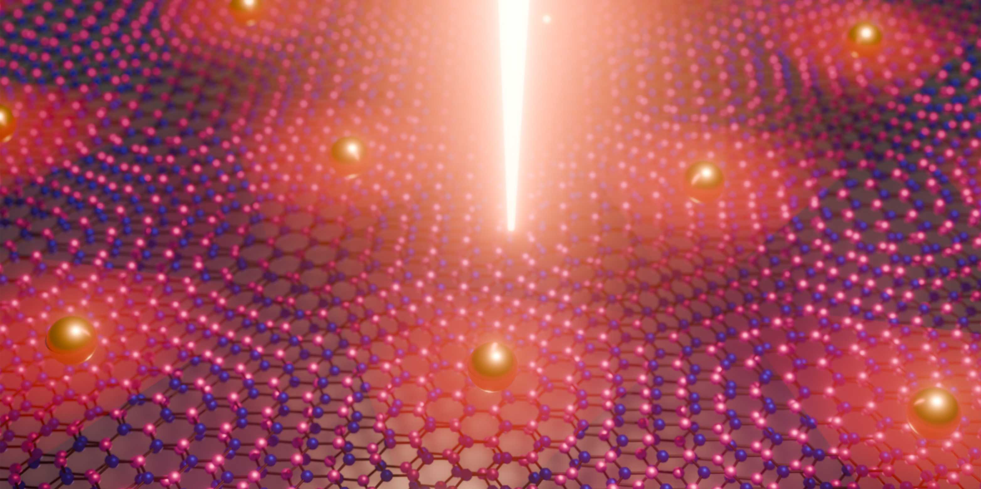
Moiré materials are produced by individually removing two layers of a material, each only one atom thick, twisting them slightly with respect to each other and then putting them back together. Since the crystal lattices of the two layers are no longer exactly on top of each other, a kind of beating effect occurs: just as two sound waves with slightly different frequencies lead to a slow periodic increase and decrease in the sound volume, in the twisted crystal lattices a "superlattice" with a much larger lattice constant arises, in which the electrons can move.

"In our new method we also produce a moiré material, but we use it in a completely different way", says Natasha Kiper, a PhD student in Imamoğlu's group. Kiper and her colleagues use two layers of hexagonal boron nitride (an artificially synthesized solid that is almost as hard as diamond) that are twisted by less than 2 degrees with respect to each other. This twisting leads to a periodic electric field that also acts at a distance beyond the material. Below the twisted boron nitride the researchers place an atomic layer of the semiconductor molybdenum diselenide. The electric field acts on the electrons inside the molybdenum diselenide and thus creates an artificial crystal lattice.
Detection using excitons
"The big advantage here is that the electric field only acts on the electrons in the molybdenum diselenide but not on the neutral excitons", says Kiper. The researchers need those excitons to study the electrons. Excitons are created when an electron in a material is excited by light of a specific frequency. As a consequence, the electron climbs to a higher energy level and leaves behind a defect, also called a hole, in the lower energy level. The negatively charged electron and the positively charged hole then attract each other and pair up to become an electrically neutral exciton.
From the light frequency at which excitons are excited the researchers were able to draw conclusions about the behavior of the electrons. By applying an electric voltage they varied the number of electrons in the semiconductor. From the exciton excitation frequency they could then, for instance, prove that when one third or two thirds of the lattice sites were filled with electrons, they arranged themselves in a regular pattern. When the number of electrons was increased further, such that more than one electron occupied a lattice site, the interactions between the electrons led to a clearly visible change in the states of the electrons. Such insights into the effects of strong interactions help physicists to understand, for instance, how certain electrical insulators can become superconductors by adding excess electrons to them.
Applicable to different materials
"Our new method is exciting also because it is highly controllable and can, in principle, be applied to many other materials", says Imamoğlu. By adding additional layers of material the strength of the electric field can be varied. Moreover, in the future it will be possible to study processes in which the electrons move between two layers. In addition to their spin, which indicates in which direction the "compass needle" of an electron is oriented, the electron would also acquire a pseudo-spin pointing up or down depending on the layer in which it finds itself. "We could use this to study exotic physical processes such as so-called chiral spin liquids, which up to now have never been observed experimentally", says Imamoğlu.
Reference
Kiper N, Adlong HS, Christianen A, Kroner M, Watanabe K, Taniguchi T, Imamoğlu A. Confined Trions and Mott-Wigner States in a Purely Electrostatic Moiré Potential, Physical Review X, 5 March 2025, DOI: external page 10.1103/PhysRevX.15.011049


