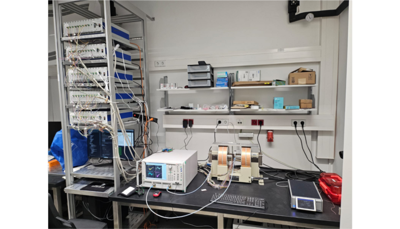
Fig. 1: Experimental inverse-design setup consisting of the device itself, mounted between the pole shoes of an electromagnet, vector network analyzer (VNA), the five multi-channel current sources, other components and a PC for running the algorithms required to solve the inverse problem. C: Noura Zenbaa, NanoMag, U of Vienna
Novel processor uses magnons to crack complex problems
An international team of researchers, led by physicists from the University of Vienna, has achieved a breakthrough in data processing by employing an "inverse-design" approach. This method allows algorithms to configure a system based on desired functions, bypassing manual design and complex simulations. The result is a smart "universal" device that uses spin waves ("magnons") to perform multiple data processing tasks with exceptional energy efficiency. Published in Nature Electronics, this innovation marks a transformative advance in unconventional computing, with significant potential for next-generation telecommunications, computing, and neuromorphic systems.
Modern electronics face critical challenges, including high energy consumption and increasing design complexity. In this context, magnonics - the use of magnons, or quantized spin waves in magnetic materials - offers a promising alternative. Magnons enable efficient data transport and processing with minimal energy loss. With the growing demand for innovative computing solutions, ranging from 5G and upcoming 6G networks to neuromorphic computing (mimicking functions of the brain), magnonics represents a paradigm shift that redefines how devices are designed and operated. Developing an innovative magnonic processor that enables highly adaptive and energy-efficient computing was a challenge that Andrii Chumak of the University of Vienna's Nanomagnetism and Magnonics Group and his collaborators successfully met.
Success Through Trial and Error
Noura Zenbaa, first author of the study, together with her colleagues around Dieter Süss, Physics of Functional Materials at the University of Vienna, built a unique experimental setup using 49 individually controlled current loops on an yttrium-iron-garnet (YIG) film. These loops created tunable magnetic fields to control and manipulate magnons. Using an "inverse-design" approach, the team allowed algorithms to determine the optimal configurations to achieve desired device functionalities, significantly streamlining the design process. After more than two years of development and testing, the team overcame many challenges. "It was a tough journey but seeing it all come together with our first successful measurement was incredibly rewarding", said Noura Zenbaa.
Creating Greener Technologies
The team's prototype demonstrated two key functions: acting as a notch filter (a component that blocks specific frequencies) and as a demultiplexer (a device that routes signals to different outputs). These capabilities are crucial for next-generation wireless communications like 5G and 6G. Unlike traditional systems, which require custom components, this versatile hardware can be adapted for various applications, reducing complexity, costs, and energy consumption. Ongoing research shows that the device can also perform all logical operations on binary data, and when scaled, it could rival traditional computers. The team plans to integrate this technology into neuromorphic computing and other advanced systems. While the current prototype is large and energy-intensive, shrinking it to under 100 nanometers could unlock exceptional efficiency, paving the way for low-energy, universal data processing and creating solutions for greener computational technologies. "This project was a bold venture with many unknowns", reflects Andrii Chumak, senior author of the study. "Yet, our initial measurements confirmed its feasibility - this concept works. Our results highlight how artificial intelligence is transforming the field of physics, much like ChatGPT is reshaping text writing and education."
Original publication:
Noura Zenbaa, Claas Albert, Fabian Majcen, Michael Kerber, Rostyslav O. Serha, Sebastian Knauer, Qi Wang, Thomas Schrefl, Dieter Suess, Andrii V. Chumak. A universal inverse-design magnonic device.
In Nature Electronics
DOI 10.1038/s41928-024-01333-7
Pictures
Fig. 1: Experimental inverse-design setup consisting of the device itself, mounted between the pole shoes of an electromagnet, vector network analyzer (VNA), the five multi-channel current sources, other components and a PC for running the algorithms required to solve the inverse problem. C: Noura Zenbaa, NanoMag, U of Vienna
Fig. 2: Experimental inverse-design setup. Component 1 - universal inverse-design device; Component 2 - electromagnet to apply a magnetic field; Component 3 - Teslameter to measure the field; Component 4 - Vector Network Analyzer (VNA) used as a microwave source and detector; Component 6 - multi-channel current sources; and Component 7 - PC to automate the setup and optimization process. C: Noura Zenbaa, NanoMag, U of Vienna
Fig. 3: The three first authors of the paper - Noura Zenbaa (on the right), Claas Abert (on the left) and Fabian Majcen (in the middle) at the moment when the universal inverse-design magnonic device was activated to solve its first problem. C: Andrii Chumak, NanoMag, U of Vienna
Fig. 4: The experimental setup. The reconfigurable inverse design device showing the 7×7 omega-shaped loop array placed on a magnetic film. It shows the local magnetic field landscape on the film, displayed in red (film top) and blue (film bottom), generated by the current applied to the loops for both current polarities. The setup includes a vector network analyzer (VNA) in combination with a power splitter and two switches. C: Noura Zenbaa, NanoMag, U of Vienna


