9 December 2024
International research team presents first electrically pumped continuous-wave semiconductor laser suitable for seamless silicon integration
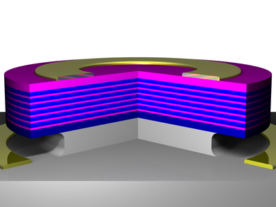
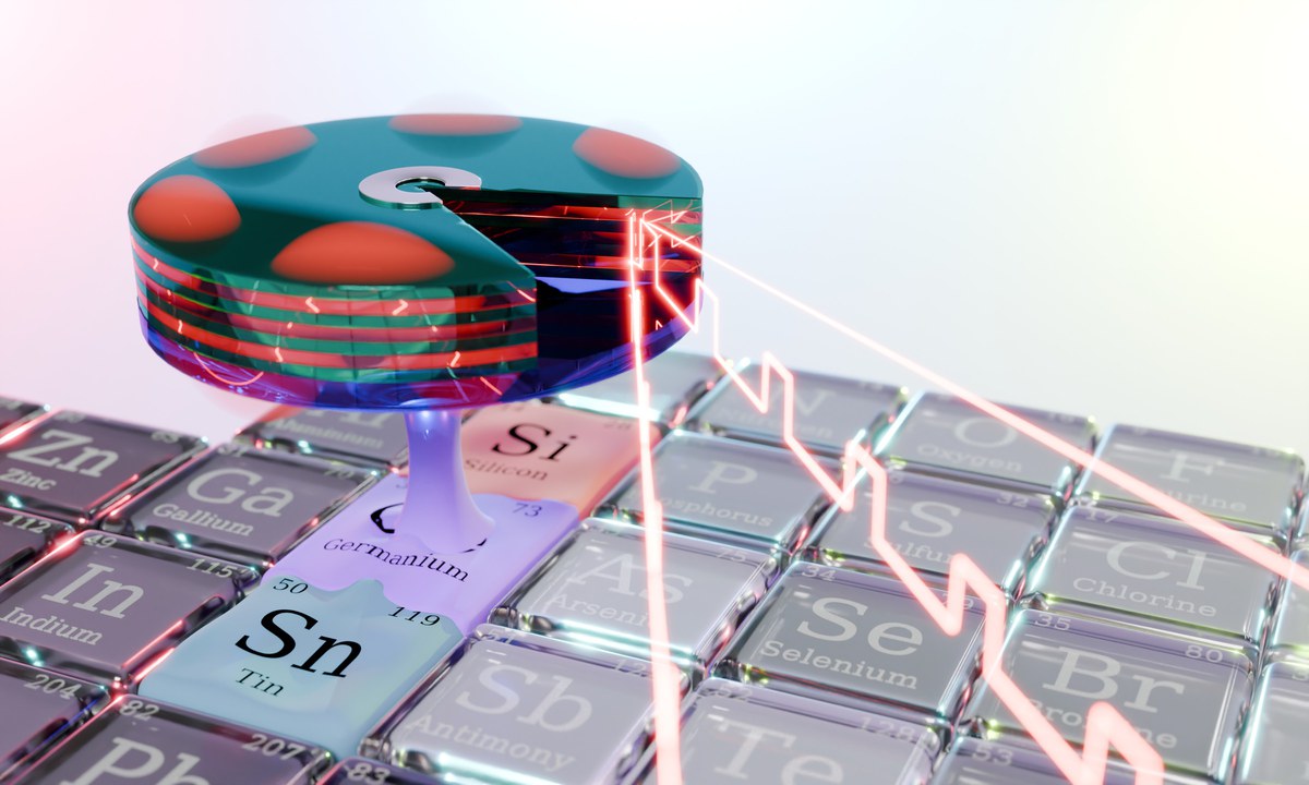
Scientists from Forschungszentrum Jülich, FZJ, the University of Stuttgart, and the Leibniz Institute for High Performance Microelectronics (IHP), together with their French partner CEA-Leti, have developed the first electrically pumped continuous-wave semiconductor laser composed exclusively of elements from the fourth group of the periodic table - the "silicon group". Built from stacked ultrathin layers of silicon germanium-tin and germanium-tin, this new laser is the first of its kind directly grown on a silicon wafer, opening up new possibilities for on-chip integrated photonics. The findings have been published in the renowned scientific journal Nature Communications.
The rapid growth of artificial intelligence (AI) and the Internet of Things (IoT) are driving the demand for increasingly powerful, energy-efficient hardware. Optical data transmission, with its ability to transfer vast amounts of data while minimizing energy loss, is already the preferred method for distances above one metre and is proving advantageous even for shorter distances. This development points towards future microchips featuring low-cost photonic integrated circuits (PICs), offering significant cost savings and improved performance.
In recent years, significant progress has been made in monolithically integrating optically active components on silicon chips. Key components, including high-performance modulators, photodetectors, and waveguides have been developed. However, a long-standing challenge has been the lack of an efficient, electrically pumped light source using only Group IV semiconductors. Until now, such light sources have traditionally relied on III-V materials, which are difficult and therefore expensive to integrate with silicon. This new laser addresses that gap, making it compatible with the conventional CMOS technology for chip fabrication and suitable for seamless integration into existing silicon manufacturing processes. It could therefore be seen as the "last missing piece" in the silicon photonics toolbox.

We have been exploring the fascinating possibilities of germanium-tin (GeSn) alloys for almost a decade. The development of an efficient, electrically pumped laser has been one of our major goals from the very beginning. This breakthrough is further proof of the enormous potential of the GeSn alloys for different applications, in this specific case for photonic applications.
For the first time, the researchers have demonstrated continuous-wave operation in an electrically pumped Group IV laser on silicon. Unlike previous germanium-tin lasers that relied on high-energy optical pumping, this new laser operates with a low current injection of just 5 milliamperes (mA) at 2 volts (V), comparable to the energy consumption of a light-emitting diode. With its advanced multi-quantum well structure and ring geometry, the laser minimizes the power consumption and the heat generation, enabling stable operation up to 90 Kelvin (K) or minus 183.15 degrees Celsius (°C).

Grown on standard silicon wafers like those used for silicon transistors, it represents the first truly "usable" Group IV laser, though further optimizations are needed to further reduce the lasing threshold and achieve room-temperature operation. However, the success of earlier optically pumped germanium-tin lasers, which have evolved from cryogenic to room-temperature operation in only few years, suggests a clear path forward.
In an optical pumped laser, an external light source is required to generate the lasing light, while the electrical pumped laser generates light when an electrical current is passing through the diode. Electrically pumped lasers are usually more energy-efficient as they directly convert electricity directly into laser light.

The research group, led by Dr. Buca from Forschungszentrum Jülich's PGI-9, has been pioneering tin-based Group IV alloys for years, collaborating with partners such as IHP, the University of Stuttgart, CEA-Leti, C2N-Université Paris-Sud, and Politecnico di Milano. They have already demonstrated the potential for applications in photonics, electronics, thermoelectric, and spintronics. With this new achievement, the vision of silicon photonics providing an all-in-one solution for next-generation microchips is now within reach.
Original publication
Seidel, L., Liu, T., Concepción, O. et al.
Continuous-wave electrically pumped multi-quantum-well laser based on group-IV semiconductors
Nat Commun (2024), DOI: 10.1038/s41467-024-54873-z


