A research team led by the Department of Energy's Oak Ridge National Laboratory has devised a unique method to observe changes in materials at the atomic level. The technique opens new avenues for understanding and developing advanced materials for quantum computing and electronics.
The new technique, called the Rapid Object Detection and Action System, or RODAS, combines imaging, spectroscopy and microscopy methods to capture the properties of fleeting atomic structures as they form, providing unprecedented insights into how material properties evolve at the smallest scales.
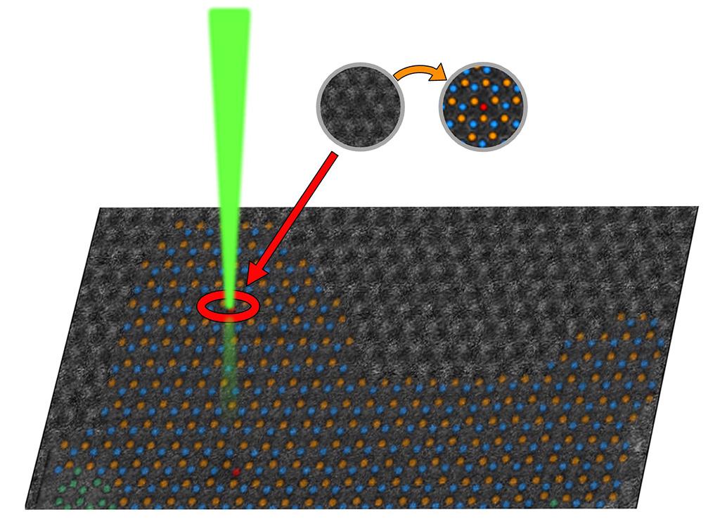
Traditional approaches combining scanning transmission electron microscopy, or STEM, with electron energy loss spectroscopy, or EELS, have been limited because the electron beam can change or degrade the materials being analyzed. That dynamic often causes scientists to measure altered states rather than the intended material properties. RODAS overcomes the limitation and also integrates the system with dynamic computer-vision-enabled imaging, which uses real-time machine learning.
When analyzing the specimen, RODAS focuses only on areas of interest. This approach enables rapid analysis - in seconds or milliseconds - compared with sometimes several minutes that can be required by other STEM-EELS methods. Importantly, RODAS extracts crucial information without destroying the sample.
All materials have defects, and these defects can directly influence virtually any of a material's properties - whether electronic, mechanical or quantum, for example. Defects can arrange themselves in a variety of ways at the atomic level, both intrinsically and in response to external stimuli, such as electron beam irradiation. Unfortunately, the local properties of these various defect configurations are not well understood. Although STEM methods can experimentally measure such configurations, investigating specific configurations without altering them is extremely challenging.
"Understanding defect configurations is crucial for developing next-generation materials," said the study's lead author, Kevin Roccapriore of ORNL's Center for Nanophase Materials Sciences. "If empowered with that knowledge, we could intentionally create a specific configuration to produce a specific property. Such work is entirely separate from the observation and analysis activity but represents one potentially impactful direction for the future."
Unleashing quantum materials' potential
The research team demonstrated their technique on single-layer molybdenum disulfide, a promising semiconductor material for quantum computing and optics applications. Molybdenum disulfide is particularly interesting because it can emit single photons from defects known as single sulfur vacancies. In this material, a single sulfur vacancy refers to the absence of one sulfur atom from its honeycombed lattice structure, which is the arrangement of the atoms. These vacancies can aggregate, creating unique electronic properties that make molybdenum disulfide valuable for advanced technological applications.
By studying molybdenum disulfide and similar single-layer materials, scientists hope to answer vital questions about optical or electronic properties at the atomic scale.
New frontier in materials science
The RODAS technique represents a significant leap forward in materials characterization. It empowers researchers to dynamically explore structure-property relationships during analysis, target specific atoms or defects for measurement as they form, efficiently collect data on various defect types, adapt to identify new atomic or defect classes in real time and minimize sample damage while maintaining detailed analysis.
By applying this technology to a single layer of vanadium-doped molybdenum disulfide, the research team gained new understanding of defect formation and evolution under electron beam exposure. This approach allows for exploring and characterizing materials in dynamic states, offering a deeper knowledge of how materials behave under various stimuli.
"Materials science techniques such as advanced electron microscopy continue to expand our comprehension of the physical world, and systems such as RODAS could play a crucial role in accelerating discovery and innovation," Roccapriore said. "The ability to observe and analyze materials at the atomic scale in real time shows potential for pushing the boundaries in computing, electronics and beyond, and ultimately enabling the development of transformative technologies."
ORNL's Laboratory Directed Research and Development program sponsored the work as part of its Interconnected Science Ecosystem, or INTERSECT, initiative. STEM experiments were supported by the DOE Office of Science Basic Energy Sciences, Materials Sciences and Engineering Division and performed at the Center for Nanophase Materials Sciences, a DOE Office of Science user facility at ORNL. This work was supported as part of the Center for the Science of Synthesis Across Scales, an Energy Frontier Research Center funded by the DOE Office of Science Basic Energy Sciences at the University of Washington.
UT-Battelle manages ORNL for DOE's Office of Science, the single largest supporter of basic research in the physical sciences in the United States. The Office of Science is working to address some of the most pressing challenges of our time. For more information, please visit energy.gov/science. - Scott Gibson


