A research group has announced a new iPMA-type Hexa-technology in Magnetic Tunnel Junctions (MTJ) that unlocks the door to improving ultra-low power in IoT edge-devices, mobile, automotive, consumer electronics, and applications operating in harsh environments, such as autonomous vehicles, industrial robots, and space applications. Crucially, the new technology is compatible with design rules for X nm generation complementary metal-oxide semiconductor (CMOS) nodes.
The Professor Tetsuo Endoh Group, from Tohoku University's Center for Innovative Integrated Electronic Systems, will present the achievement at the "2022 IEEE International Electron Device Meeting," one of the most prestigious international conferences on electron devices, which will be held in San Francisco from December 3 to 7, 2022.
Innovative AI and LSI are indispensable for realizing Society5.0 and carbon neutrality by 2050. In Society5.0, all objects and humans will be connected via IoT; necessary information will be obtained instantaneously using AI, and that information will enhance human convenience. However, to achieve these targets, data must be processed instantly using edge devices, most of which are powered by batteries. In order not to sacrifice user convenience, low power consumption is essential for edge devices. Therefore, researchers have turned to logic circuits embedded with Spin Transfer Torque Magnetoresistive RAM (STT-MRAM) technology, owing to its low power consumption and high performance.

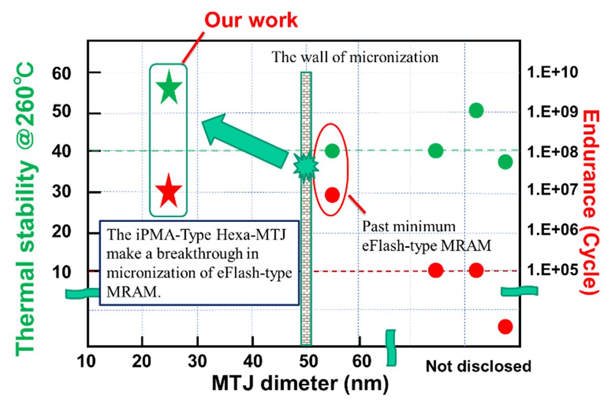
Two types of MRAM - one for SRAM and the other for eFlash replacement - have been developed. Yet, scaling problems exist with eFlash-type MRAM; eFlash-type MRAM requires a higher thermal stability factor because data must be retained during a solder reflow process at 260 °C. This problem is compounded since the thermal stability factor is proportional to the recording layer volume and inversely proportional to the absolute temperature.
Two ways to solve this dilemma have been proposed: shape anisotropy MTJ and multilayered iPMA-type MTJ. Shape anisotropy MTJ is a promising candidate for attaining a high thermal stability at junction sizes below 20 nm. However, it faces a device design problem, specifically the narrow selectivity of the MTJ diameter. Conversely, the iPMA-type MTJ can continuously obtain high thermal stability without significantly changing the material and the MTJ patterning process. The high thermal stability in the iPMA-type MTJ can be controlled continuously by adjusting the number of CoFeB/MgO interfaces and the free layer thickness. It enables seamless scaling and solder reflow capability with back-end-of-line (BEOL) process compatibility. The diameter of MTJ formed in the BEOL process must be fabricated less than 30 nm to satisfy the design rule of X nm CMOS node.
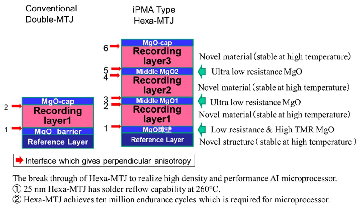
Professor Endoh's group developed iPMA-type Hexa-interface MTJ (Hexa-MTJ) with the four technologies below:
- Novel low resistance area product (RA) MgO technology
- A low temperature dependence of the recording layer
- A low damage fabrication process
- A stable reference layer
Moreover, the Hexa-MTJ technology successfully accomplished the following:
- More than twenty years of data retention characteristics
- A solder reflow capability
- Endurance reached at least 1 X 10⁷ cycles
"We are the first to realize these severe conditions for the 25 nm MTJ," said Professor Endoh. "The 25 nm iPMA-type Hexa-MTJ is a large-capacity STT-MRAM technology that satisfies the BEOL design rules for X nm generation CMOS semiconductor processes and can replace eFlash for X nm generation CMOS logic."

Thanks to the group's breakthrough, STT-MRAM's application scope can now be expanded to leading-edge logic, enabling ultra-low-power consumption, excellent scalability, and high reliability of application processors in a wide range of fields, such as IoT, AI, and harsh environmental applications.
This work was supported by CIES's Industrial Affiliation on STT-MRAM program, NEDO JPNP12004, and X-NICS of MEXT JPJ011438.

- Publication Details:
Title: 25 nm iPMA-type Hexa-MTJ with solder reflow capability and endurance > 107 for eFlash-type MRAM
Authors: H. Honjo, K. Nishioka, S. Miura, H. Naganuma, T. Watanabe, T. Nasuno, T. Tanigawa, Y. Noguchi, H. Inoue, M. Yasuhira, S. Ikeda, and T. Endoh
Conference: IEEE International Electron Device Meeting


