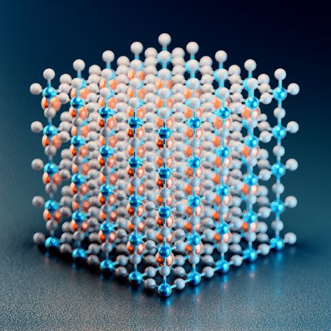
Figure 1: Illustration of an idealized structure of a perovskite. RIKEN researchers arranged cubic nanoparticles of a perovskite on a coated surface and investigated their properties. © OCLUSTERING/SCIENCE PHOTO LIBRARY
In a demonstration that unlocks exciting possibilities for solar cells and light-emitting diodes (LEDs) based on materials known as perovskites, RIKEN researchers have refined techniques for controlling the optical and electronic properties of perovskite nanocrystals1.
The high tunablity of all-inorganic nanocrystals made from perovskite materials with the chemical formula CsPbX3 (where X is a halide such as chlorine, bromine or iodine) make them attractive for use in various applications including bioimaging, LEDs, lasers and electronic devices.
Nanocrystals of various shapes have been investigated including nanorods, nanowires and nanoplatelets. The properties of these nanocrystals vary depending on their direction. In contrast, cubic nanocrystals have higher symmetry, with all their faces being the same.
However, if cubic nanocrystals are arranged in a single layer on a flat surface, their four side faces will be identical, but their top faces will be exposed to air, while their bottom faces will contact the substrate. The effect of this difference in faces on their properties has been little studied until recently.
Now, Retno Miranti of the RIKEN Center for Emergent Matter Science and co-workers have manipulated the electronic states in cubic nanocrystals of cesium lead bromide (CsPbBr3) by arranging them on a coated substrate.
The team, led by Yong-Jin Pu, coated quartz substrates with 3-aminopropyltrimethoxysilane (APS) and then assembled cesium lead bromide nanocrystals in a single layer. Using a dip-coating technique, they were able to cover 99% of the surface.
"The toughest challenge was achieving uniform coating of nanocrystals across the surface of the substrate without any aggregation or uneven dispersion," notes Miranti.
The APS-treated substrates bonded with the bottom face of each nanocrystal, disrupting the material's symmetry. This interaction caused their electronic states to be vertically aligned in a process that exceeded the team's expectations.
"We were surprised to find that the amino groups played a dual role," Miranti notes. "They both improved adhesion and altered the orientation of the transition dipole moments in a monolayer."
Substrates treated with other silane agents could not achieve the same level of uniformity or anisotropic behavior, highlighting the role of APS treatment in enabling precise control.
Aligned transition dipole moments achieved through this method have significant implications for device performance.
In LEDs, the alignment of transition dipole moments enables precise control of light polarization, enhancing display technology. In solar cells, it optimizes light absorption. "This increases the light-harvesting efficiency, crucial for increasing the power conversion efficiency of solar cells," says Pu.
Pu's team plan to explore energy transfer within nanocrystal assemblies, aiming to unlock further advances in optoelectronic engineering.

Retno Miranti (third from left), Yong-Jin Pu (far right) and colleagues have developed techniques to align nanocrystals by breaking their symmetry. © 2025 RIKEN


