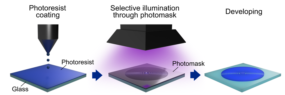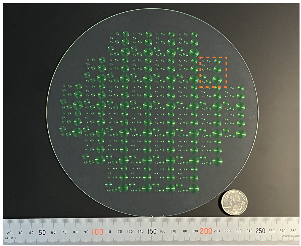


Paper-thin optical lenses simple enough to mass produce like microchips could enable a new generation of compact optical devices. A team with researchers at the University of Tokyo and JSR Corp. fabricated and tested flat lenses called Fresnel zone plates (FZPs), but did so for the first time using only common semiconductor manufacturing equipment, the i-line stepper, for the first time. These flat lenses currently lack the efficiency of in-production lenses, but have the potential to reshape optics for industries ranging from astronomy to health care and consumer electronics.
Flat lenses, such as metalenses, exist, but they come with hefty price tags and a high degree of complexity, and only a small number of devices are available. In the race to increase the quality, performance and efficiency of devices whilst reducing costs, manufacturers, through the work of academic researchers, seek alternatives. FZPs have become a good candidate to improve optical devices where space is critical. And for the first time, researchers crafted sample lenses with just a few straightforward steps using industry standard machinery.
"We developed a simple and mass-producible method for FZPs using a common semiconductor lithography system, or stepper," said Associate Professor Kuniaki Konishi from the Institute for Photon Science and Technology. "This is due to a special type of photoresist or mask called a color resist, which was originally designed for use as color filters. By simply coating, exposing and developing this material, we produced lenses capable of focusing visible light down to only 1.1 microns, around 100 times thinner than a human hair."
The current drawback with the new FZPs is that they only have a light-gathering efficiency of 7%, meaning they produce excessively noisy images. But already the team is working on ways to increase this fourfold by changing the way they use the color resists. However, this would require a greater degree of control over the color resists' physical properties than was afforded the researchers at the time of this study, though the ability to do this does exist.
"In addition to efficiently fabricating FZPs, we also devised simulations which are confirmed to match our experiments very tightly. What this means is, we could tailor designs to match specific applications in different fields, such as medicine, before committing to production," said Konishi. "Furthermore, we envisage environmental and economic benefits too, as unlike traditional manufacturing methods, the FZP production process eliminates the need for toxic etching chemicals and significantly reduces energy consumption."
So, it might be a while before FZPs help you capture moments in high visual fidelity with your ultrathin smartphone, but this, or technology inspired by it, will likely come along soon.


